Electron Beam Lithography System ELS-BODEN Σ
New
Nanofabrication System
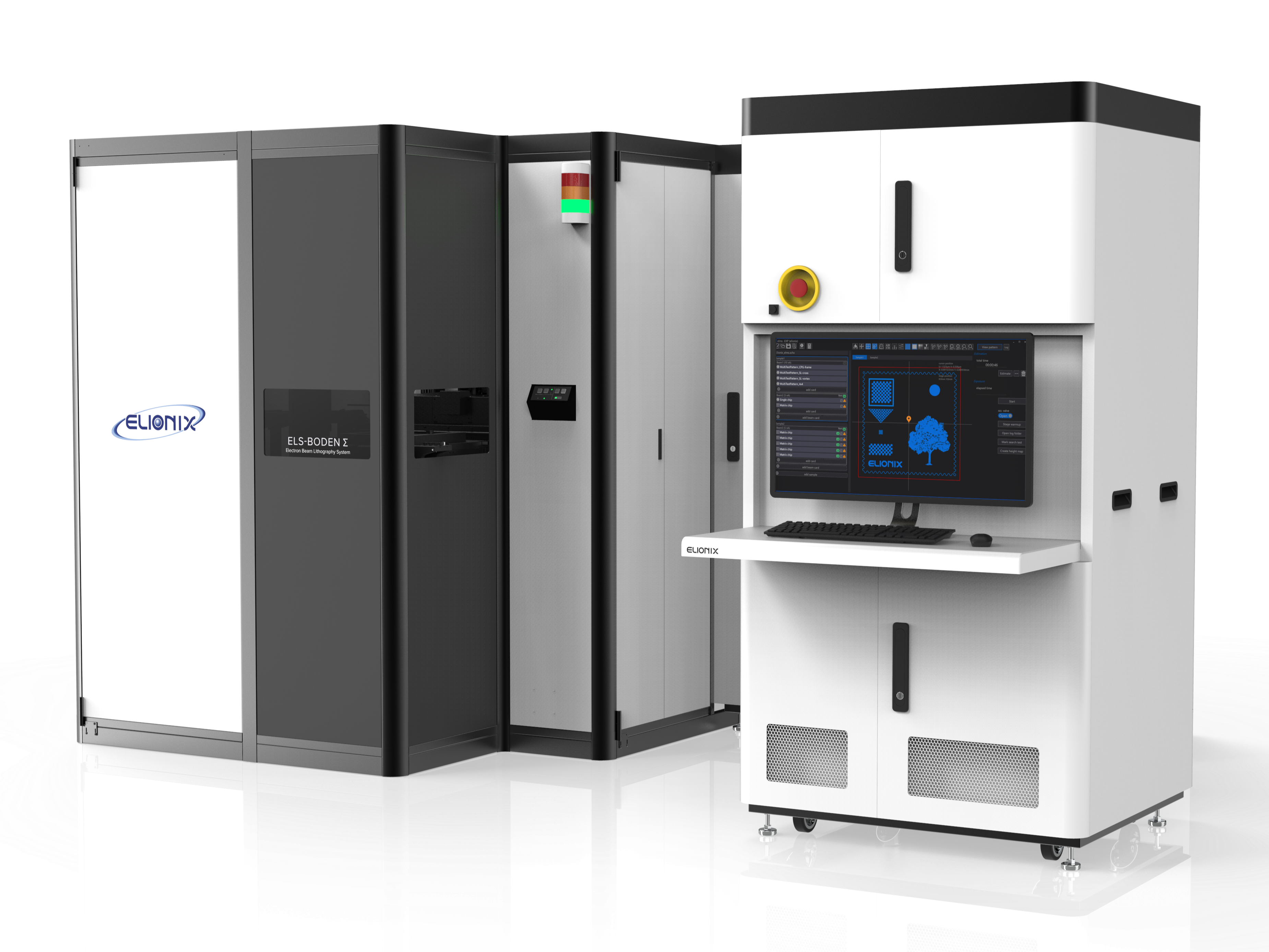
This is the latest model of the electron beam lithography equipment that we have been working on for many years since our founding. Adopting a module system, you can freely combine the acceleration voltage, chamber size, transfer mechanism, and anti-vibration table to build the optimum unit for each application.
It is possible to expose the entire surface of a 12 inch wafer.
By docking with the wafer automatic transfer system (EFEM), multi-stage processing by robots is possible.
Accelerating voltage can be selected from 50, 100, 125, 150 kV depending on the application.
By selecting a high-current model with a maximum current of 800 nA, high-throughput microfabrication that exceeds the common sense of electron beam lithography is possible.
ELS-BODEN Series Lineup

Fastest in the world!
High-speed scanning with a scan clock of 400 MHz and a high-speed stage can also be used for production.
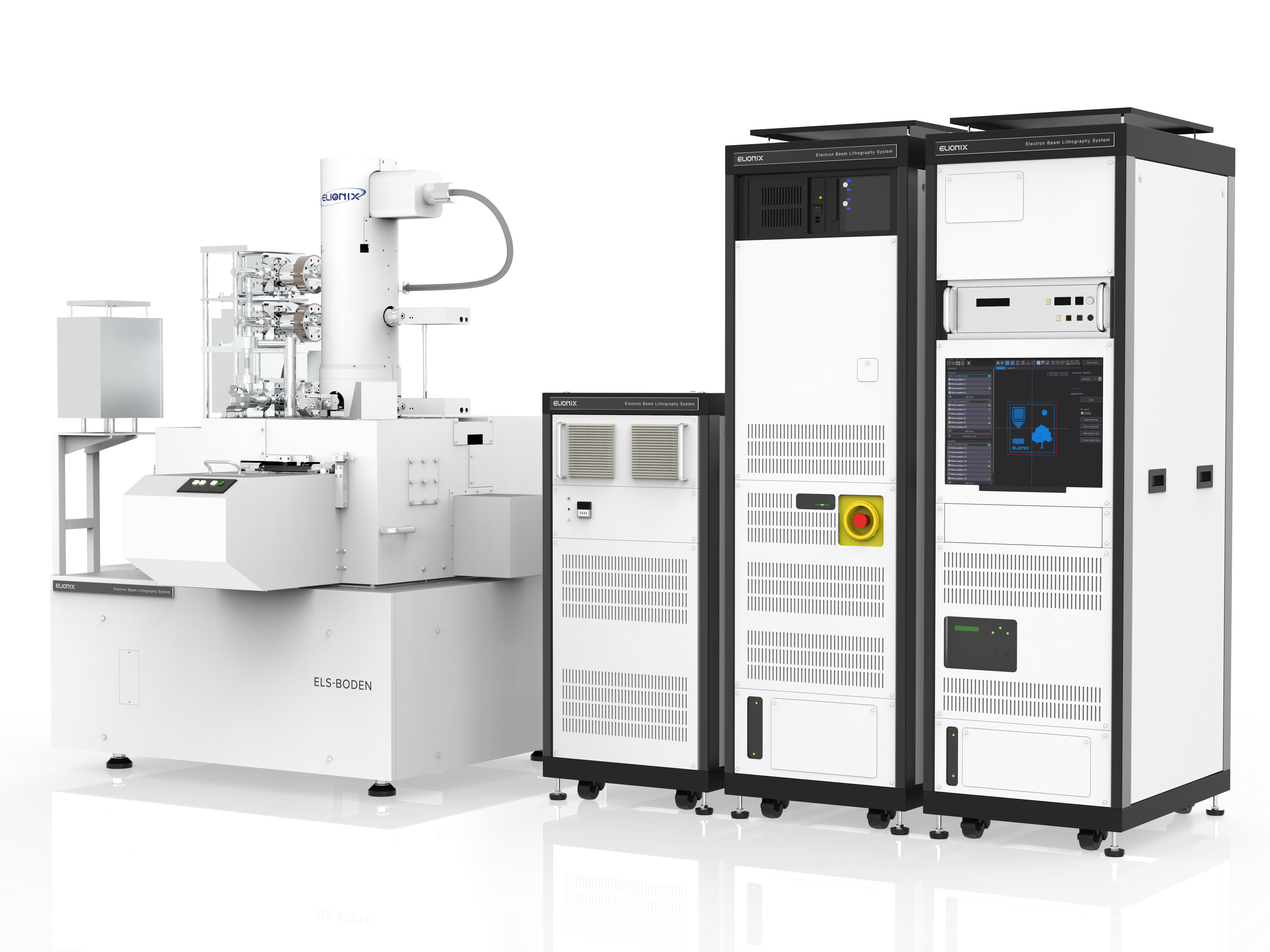
Perfect for research and development!
Supports a wide range of applications from high-definition drawing to high-current high-speed drawing
Electron Beam Lithography System ELS-ORCA
New
Nanofabrication System
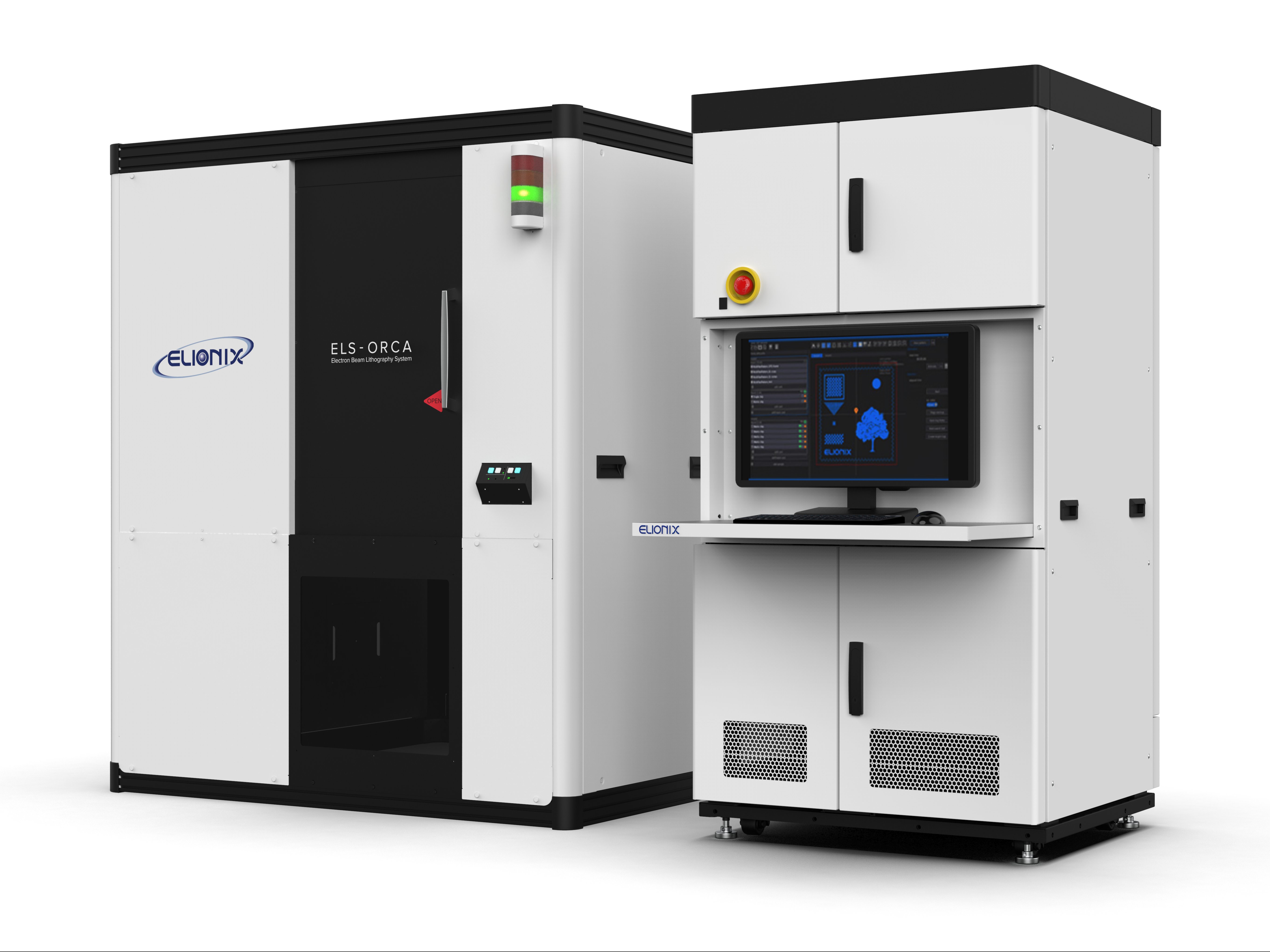
The latest entry model of electron beam lithography system for R&D
Customizable with various options
User-friendly software "elms"
Enclosure to reduce external disturbances
Retarding system for low-damage/high-resolution SEM observation
The Best Choice for R&D!
The standard acceleration voltage is set at 30 kV and can be customized with various options
Electron Beam Lithography System ELS-HAYATE
New
Nano Fabrication System
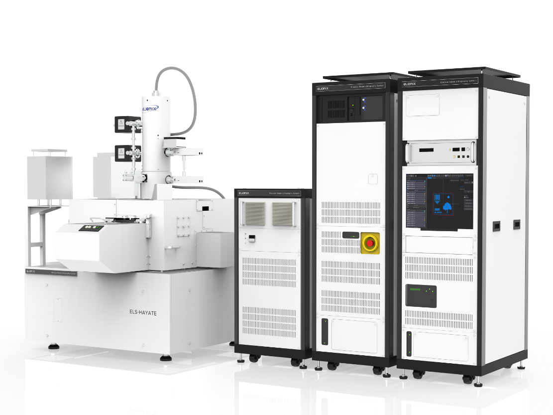
Achieved Ultra-High-Throughput Electron Beam Lithography that overturns common sense.
A one-shot writing with a maximum field size of 5 mm is possible.
Equipped with a high-current model with a maximum current of 800 nA, high-throughput microfabrication beyond the common sense of electron beam lithography is possible.
Equipped with a high-speed scan system with the industry's fastest scan clock of 400 MHz.
Full exposure of 12-inch wafers is possible.
By docking with the wafer automatic transfer system (EFEM), multi-stage processing by robots is possible.
Industry Largest!
Achieved the industry's largest 5 mm deflection. It is ideal for applications where you are concerned about stitching errors between fields.
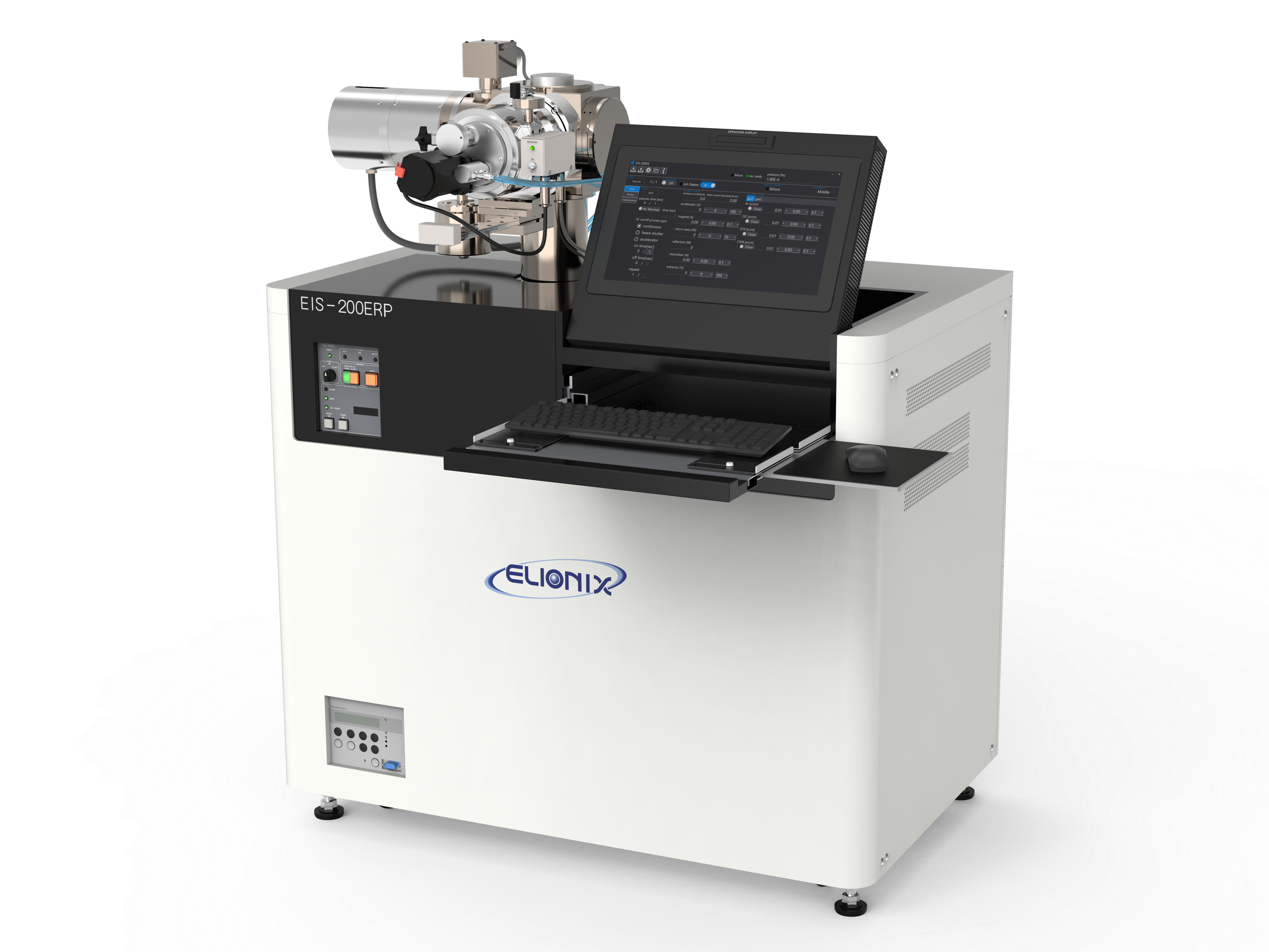
The Electron Cyclotron Resonance (ECR) type ion beam realizes etching with minimal damage to the mask. The compact model can also be used for film deposition applications.
An ion beam accelerated in a vacuum enables highly straight etching.
Active gases such as O2 and CF4 can also be used, and reactive ion beam etching (RIBE) is also possible.
Based on PC operation, process control can be easily performed.
Various options are available for the compact model, and it can also be used as a ion beam sputtering deposition (IBSD) system.
EIS Series Lineup

Compact but high performance!
Nano-scale etching and deposition are possible using ECR ion beams.
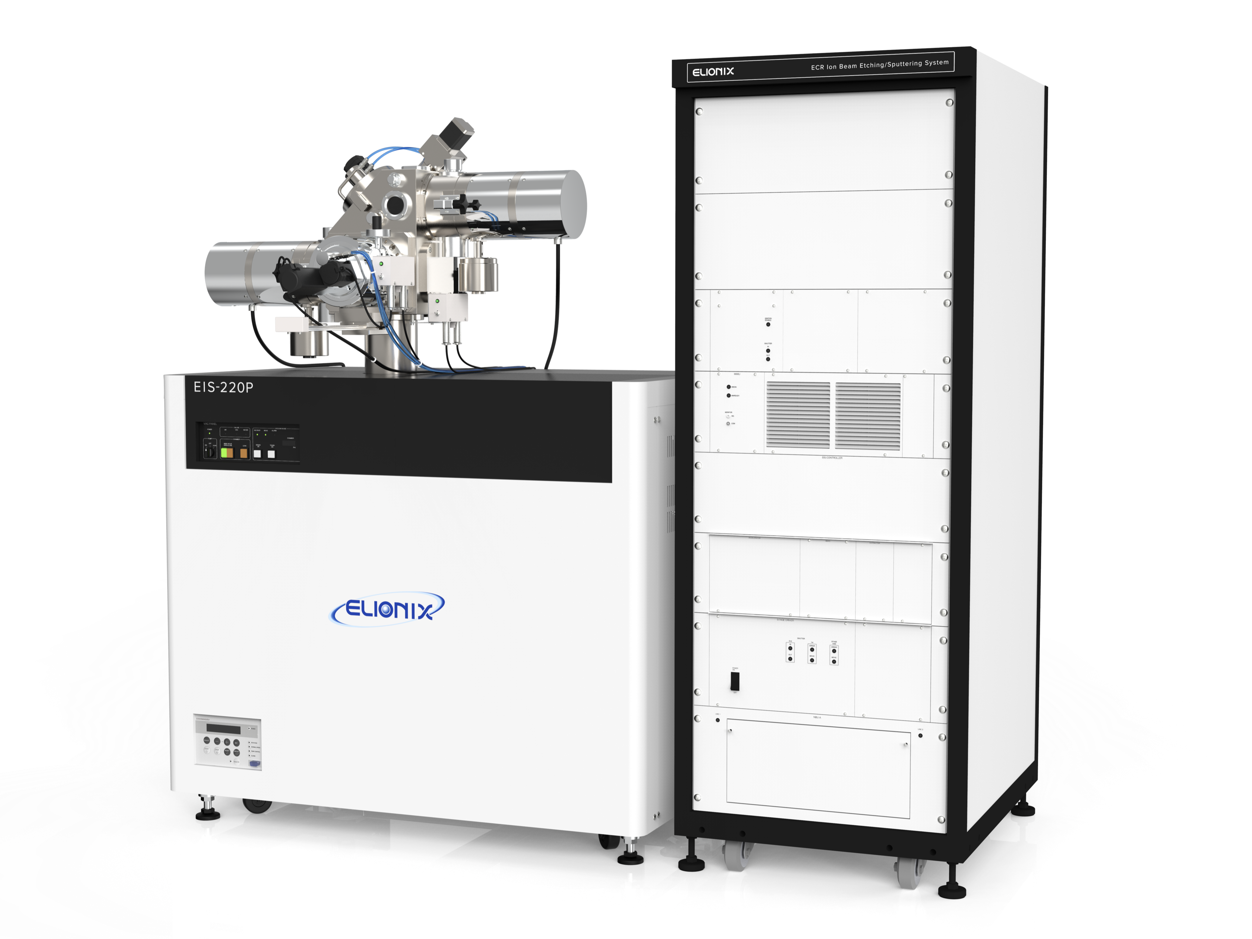
Equipped with two Ion Guns!
Etching and deposition can be repeated without breaking the vacuum with two ion guns.
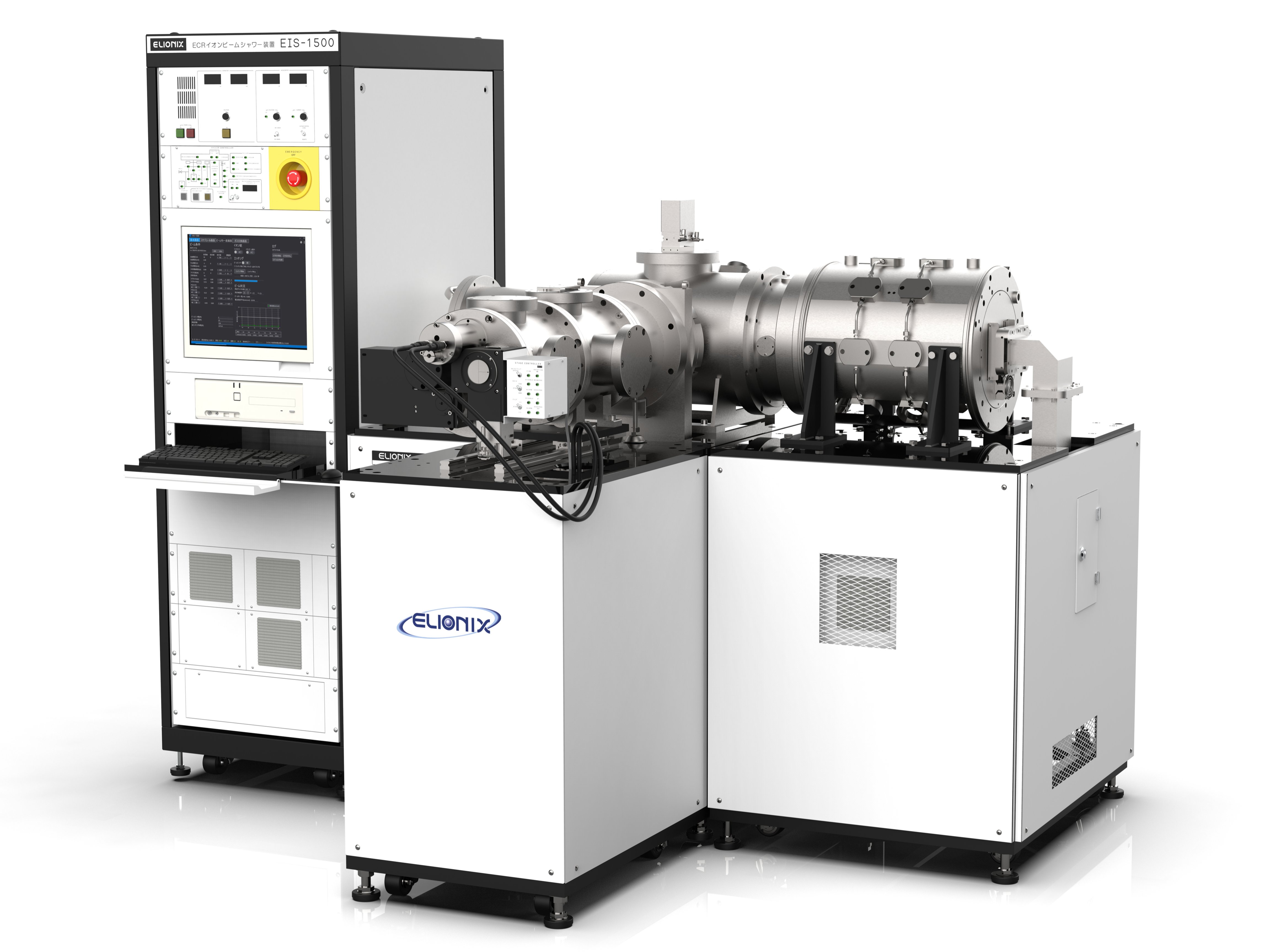
Ø108 mm Large diameter beam!
Anisotropic dry etching is possible by making full use of the beam in-plane distribution monitoring function.
Sales Headquarters (Hachioji City, Tokyo)
TEL: +81-42-626-0611
Hours: Monday-Friday 8:30-17:30
Except Weekends, National Holidays, and Year-end and New Year Holidays
