
Electron Beam Lithography System ELS-BODEN
New
Nano fabrication System
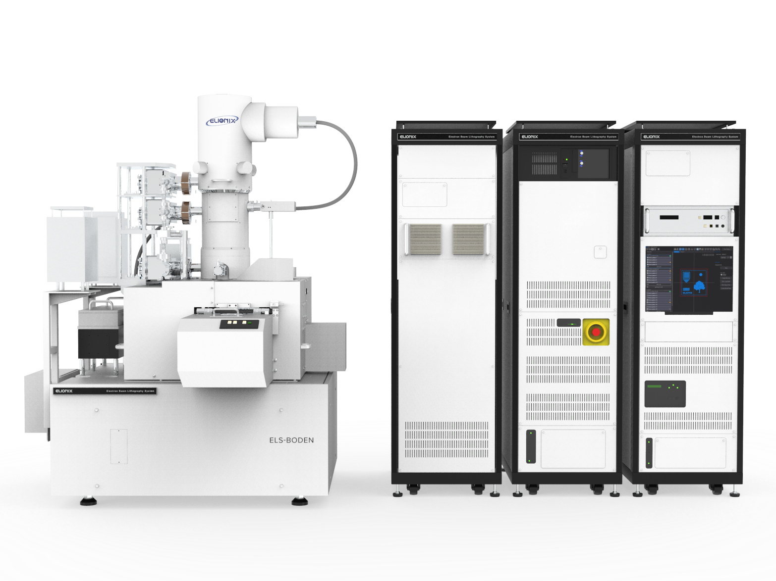
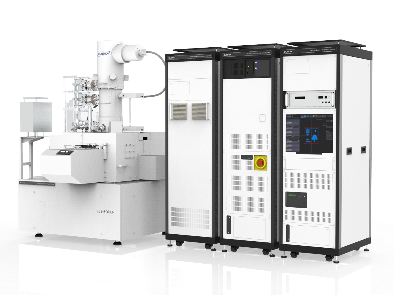
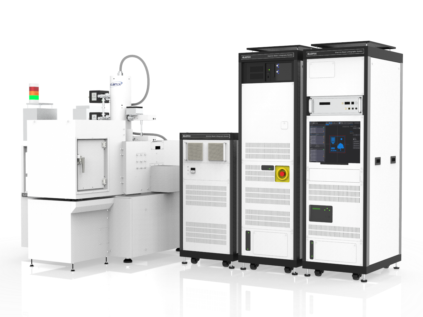
8” and 12” Lineup
World’s first full 12” exposure capability. Supports sizes from small pieces, often used in R&D, to 2, 3, 4, 5, 6 , 7, 8, and 12 inch wafers as well as mask blanks in 6025 and 9025 size.
Automatic Loading System
Single autoloader, suitable for R&D applications, multi autoloader, for low-volume to middle-volume production and robot loader are available depending on your needs.
Simple GUI Software
New software “elms” is included as standard with the lithography system. Since each of the packages, CAD conversion, beam adjustment, exposure, and SEM observation, is independent, it makes the program intuitive and your workflow more efficient. Access to each function can be restricted for different users by using account management function.
| TFE Filament | ZrO/W Thermal field emitter | ||||
|---|---|---|---|---|---|
| Acceleration Voltage | 50 kV | 100 kV | 125 kV | 150 kV | |
| Beam Current | 1 nA ~ 800 nA | 20 pA ~ 100 nA | 5 pA ~ 100 nA | 5 pA ~ 100 nA | |
| Minimum Beam Diameter | Ø 2.8 nm | Ø 1.8 nm | Ø 1.7 nm | Ø 1.5 nm | |
| Standard Field Size | 1000 μm□ | 1000 μm□ | 500 μm□ | 500 μm□ | |
| Min./Max. Field Size | Min. 100 μm □ Max.(Option)3000 μm□ | ||||
| Scan Clock | Max. 100 MHz | ||||
| Shot Pitch | Min. 0.2 nm | ||||
| Max. Sample Size | 8” Wafer / 12” Wafer | ||||
| Max. Exposure Area | 200 mm x 200 mm / 300 mm x 300 mm | ||||
| Loading Mechanism | Single AutoLoader Multi AutoLoader Robot Loader | ||||
| Software | elms • Beam adjustment function • Drawing schedule function • Pattern data conversion function • Account management • Python scripting | ||||
Sales Headquarters (Head Office: Hachioji City, Tokyo)
Hours: Monday-Friday 8:30-17:30
Except Weekends, National Holidays, and Year-end and New Year holidays