
Technical Information: Electron Beam Lithography Systems [Beginner Level]

What is an electron beam lithography system?
An electron beam lithography system is an extremely precise exposure device used in electron beam lithography (EBL).
Just as conventional printing and photography use “light” to imprint images, this system uses a “beam of electrons” to freely expose ultra-fine patterns on the nanometer (one-millionth of a millimeter) scale.
“Super-precise printer for the nano world,” indispensable for creating structures too small to be seen with the naked eye—such as those found in cutting-edge modern technologies, including high-speed smartphone CPUs and the core components of quantum computers.
Why “electrons” instead of “light”?
When creating nanoscale patterns, the biggest obstacle is a phenomenon known as “light diffraction.”
- The Limits of Light (Diffraction Limit):
The “light” used in standard exposure processes exhibits wave-like properties, and features smaller than the wavelength of light (several hundred nanometers) become blurred and cannot be accurately reproduced. This is known as the “diffraction limit.” - The Advantages of Electrons:
On the other hand, high-speed, accelerated “electrons” behave as particles with wavelengths that are overwhelmingly shorter than those of light (0.01 nanometers or less).
By utilizing this characteristic of “extremely short wavelengths,” it becomes possible to focus the beam to an extreme fineness of a single nanometer (1 to less than 10 nanometers)—a level of precision that light can never achieve.
Even intricate circuits that are too fine to be drawn with a “light pen” can be drawn with exquisite precision using an “electron pen.” This is why electron beam lithography systems are indispensable for the development of next-generation devices.
How Electron Beam Lithography Works
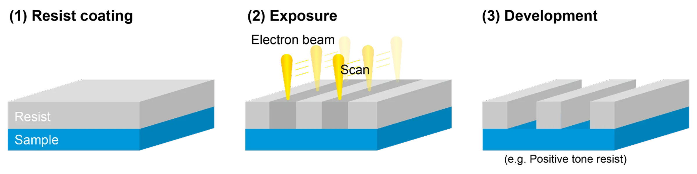
Pattern formation using electron beam lithography (EBL) is broadly carried out in the following three steps.
- Resist coating: First, a photosensitive material called a resist is applied to the sample.
- Electron beam irradiation: Next, an electron beam is irradiated to break the main chains of the resist (in the case of positive-type resist) or to cross-link them (in the case of negative-type resist).
- Development: Finally, by immersing the sample in a developer solution, the irradiated (or non-irradiated) areas are dissolved, forming the desired fine pattern.
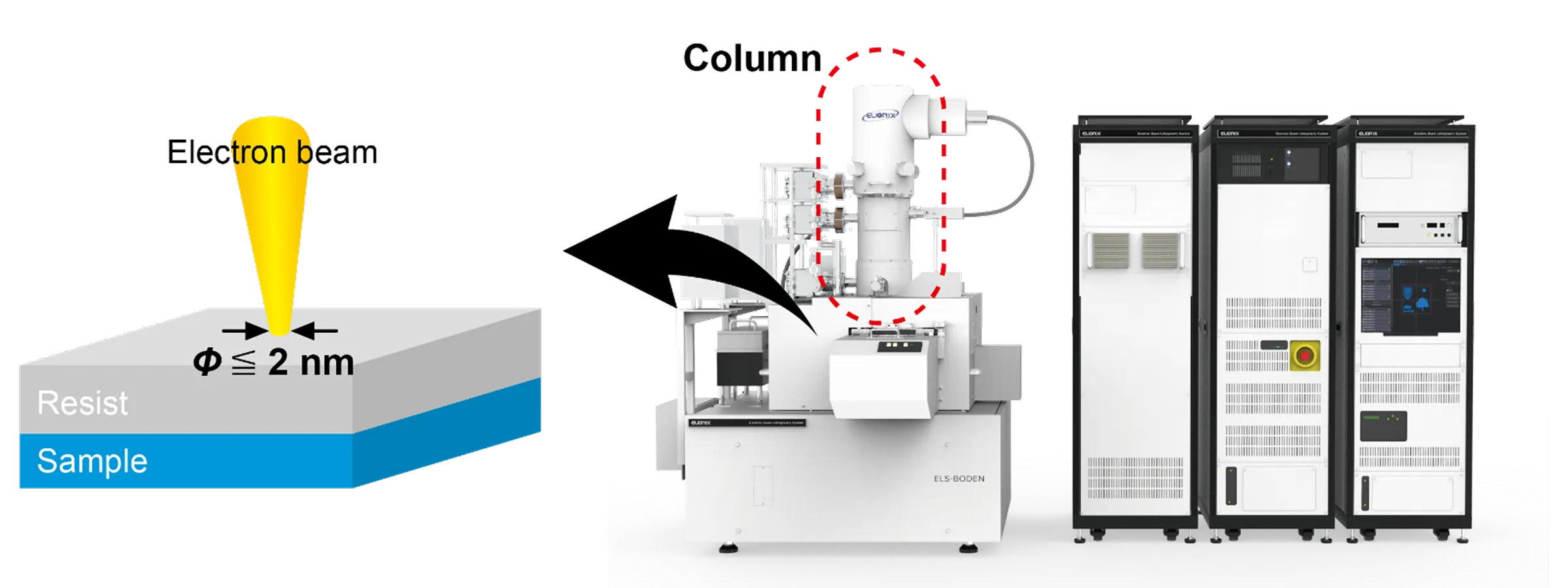
The Column: the key component enabling fine detail
In the “electron beam irradiation” process described above, the “column” plays a pivotal technical role.
Inside the column are an “electron gun” that emits electrons, an ‘accelerator’ that accelerates the electrons, and an “electron optical system (electromagnetic lenses)” that focuses and bends the beam.
The electron beam accelerated in the upper part of the column is focused to an extremely fine diameter of 2 nm or less through advanced lens control technology cultivated by Elionix over many years. By freely scanning this ultra-fine electron beam, it becomes possible to form intricate patterns with high resolution on the order of a single nanometer.
What the Elionix System Can Do (Features)
Elionix's electron beam lithography systems enable microfabrication using core technologies cultivated over half a century.
Ultra-fine machining at the single-nanometer level
Thanks to our advanced electro-optical design capabilities, we can achieve a minimum beam diameter of 2 nm or less. Our high-end models achieve a minimum beam diameter of 1.5 nm (for the 150 kV acceleration voltage). This enables us to meet the extremely demanding microfabrication requirements at the 3 nm level.
Support for a wide range of sample sizes and automated handling
We offer flexible support for a wide range of materials, from small-sized samples commonly used in research and development to wafers and mask blanks up to 12 inches in size. Furthermore, our comprehensive lineup of automated handling systems—ranging from single auto-loaders to multi-auto-loaders and robotic loaders—seamlessly covers everything from small-scale research prototyping to medium-volume production.
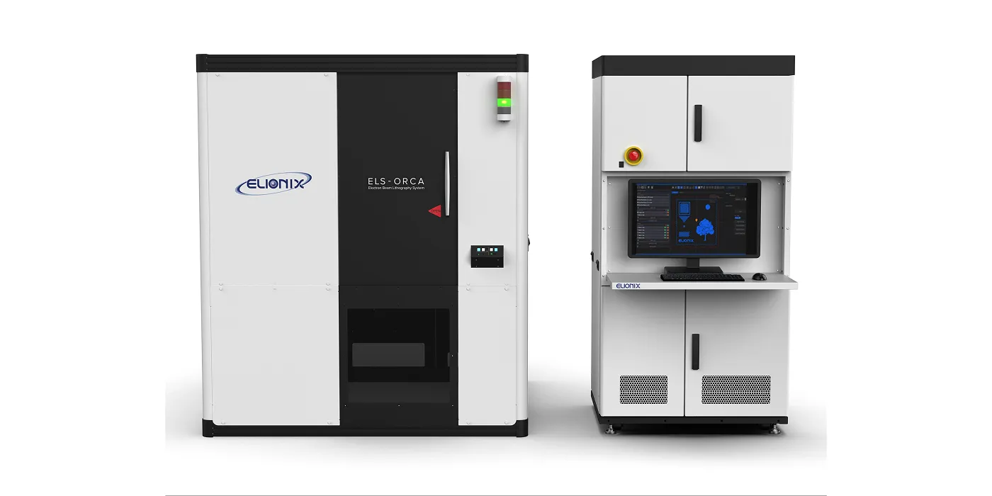
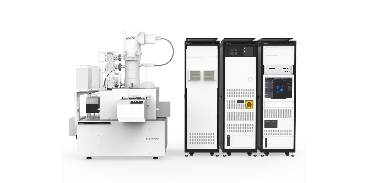
A product lineup covering everything from research to production
ELS-ORCA
ELS-BODEN
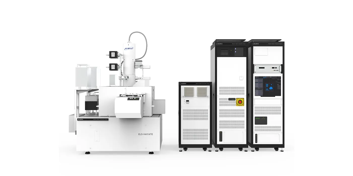
ELS-HAYATE
A Future Powered by Elionix Technology (Applications)
The fine patterns produced by electron beam lithography have become indispensable to today’s cutting-edge technology. They are primarily used in a wide variety of fields, including the following:
- Semiconductor Integrated Circuits:Prototyping and verification of next-generation chips
- Quantum Computers: Fabrication of microstructures required for qubit formation
- Power Electronics:Gate structures for next-generation power devices
- Optical Devices:Optical components such as metamaterials and photonic crystals
- Biotechnology and New Materials:Research on nanofluidic devices and metamaterials
Elionix's equipment serves as the foundation for innovation in these fields and is being utilized to pave the way for the future of science and technology.