
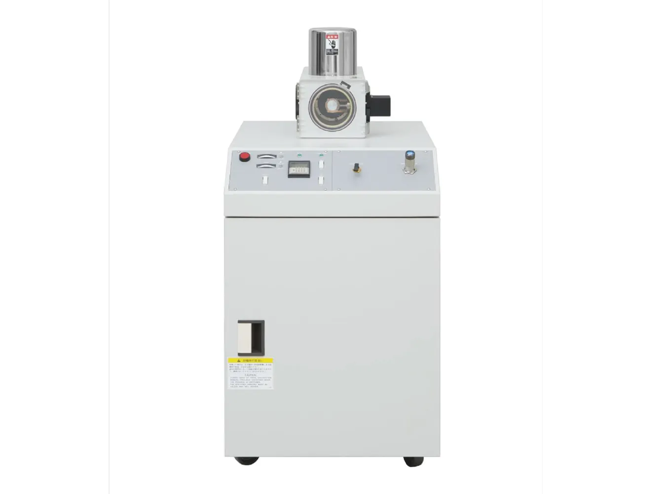
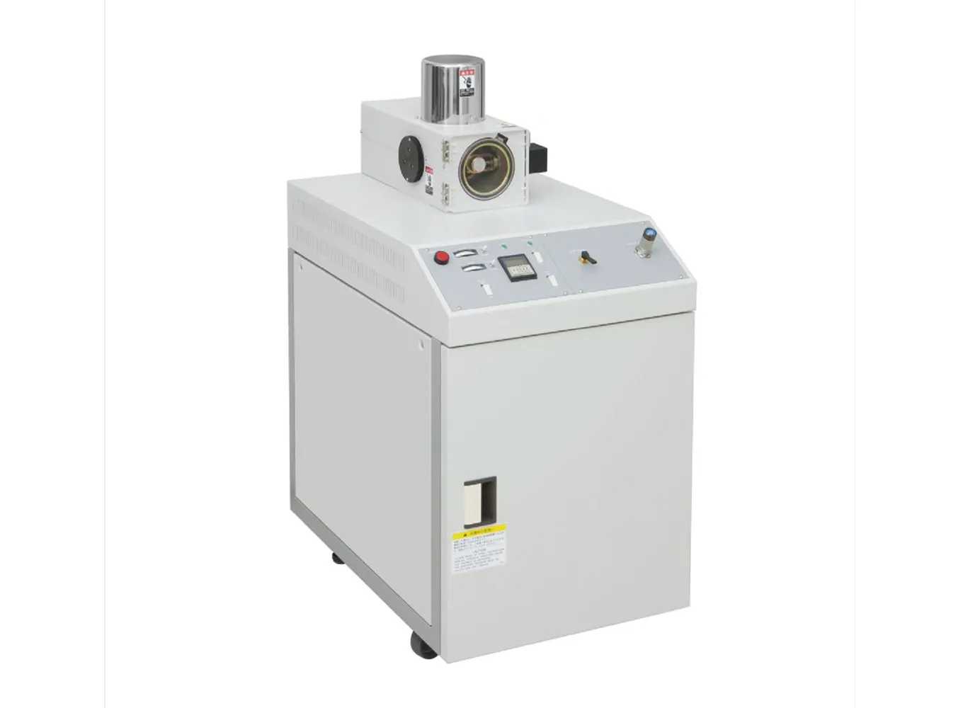
Superfine Coater
ESC-101
Superfine Coater
ESC-101
- Measurement and Analysis Equipment
Sample Coating System for High-Resolution SEM
Key Features
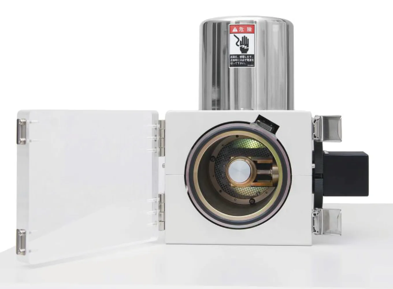
By adopting a proprietary new type of ion gun that combines a hollow-anode ion gun with a magnetron ion gun,
we have succeeded in producing ultra-fine-structure tungsten films.
For samples prone to significant charging, the time and effort required for SEM observation at extremely low acceleration voltages are immeasurable.
Furthermore, charge contrast is extremely difficult to interpret.
With this system, it is possible to safely and quickly obtain dense, highly conductive films of tungsten sputter particles—which are difficult to observe at SEM resolution.
*As a conductive coating material, tungsten excels in both electrical conductivity and secondary electron yield in the low acceleration voltage range.
You can easily apply a coating using ultrafine tungsten particles with a particle size of 1 nm or less.
- The particle size of tungsten films deposited using Ar-ion beam sputtering ranges from 0.2 nm to 0.5 nm. Even under SEM observation at 700,000× magnification, no granularity is observed, making it ideal for high-magnification observation.
- Since the sample surface temperature remains below 50°C, coating can be performed with minimal thermal damage.
- Coating can be completed in a short time (3–5 minutes after reaching a vacuum of 1 Pa).
- The coating adheres well to curved surfaces and provides excellent coverage and adhesion even in narrow gaps. A coating film that resists contamination can be obtained.
- While tungsten is the standard target material, we can switch to various other target materials upon request.
*Option: Etching is also available.
App Gallery
TEM image: Limited-field electron diffraction pattern
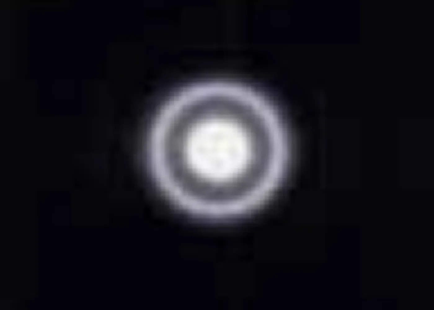
W film deposited using ESC-101, film thickness 15 nm,
TEM image, magnification 1,000,000×
It can be seen that the deposited tungsten film is in an amorphous state.
TEM image, magnification 1,000,000×
It can be seen that the deposited tungsten film is in an amorphous state.
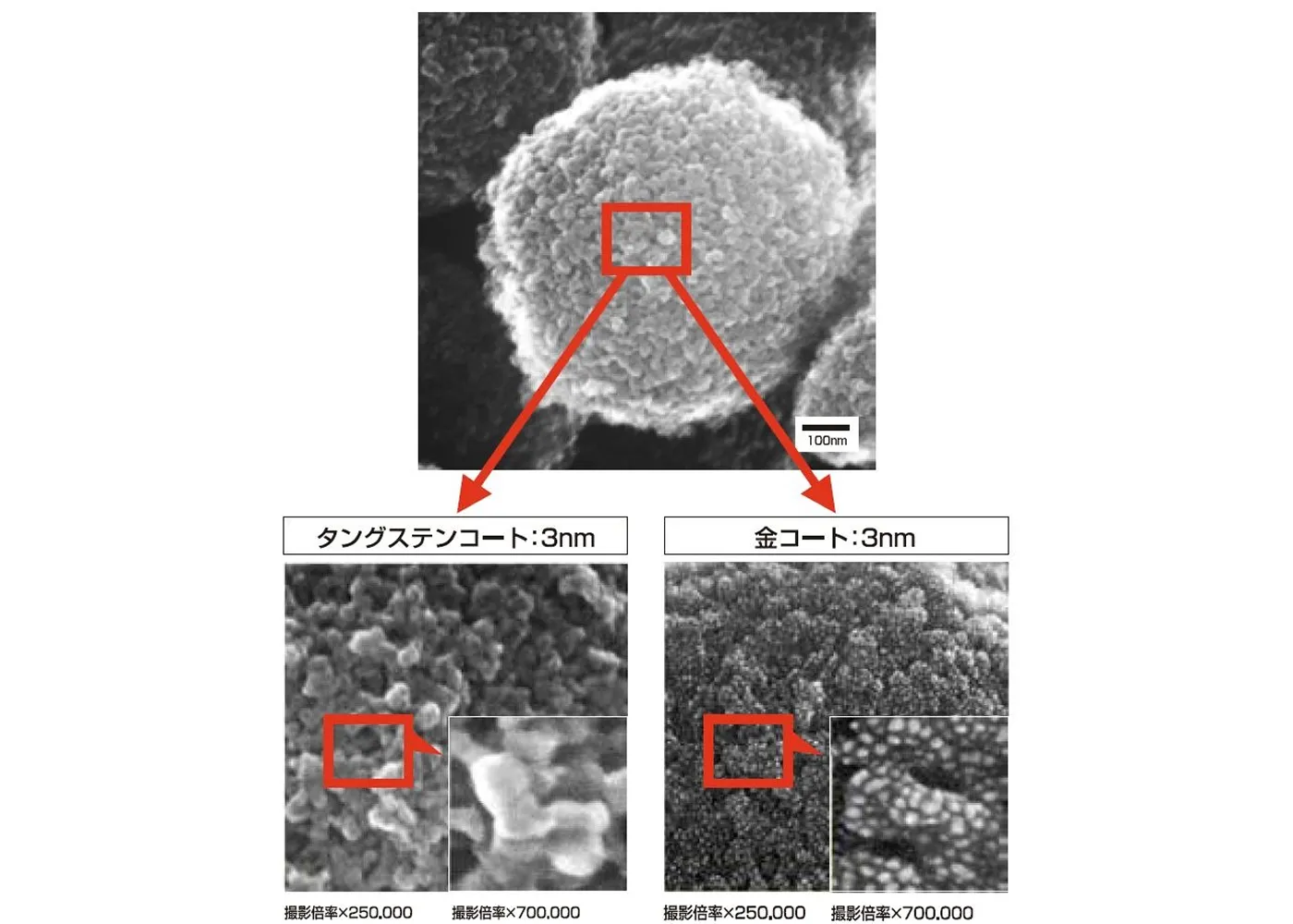
Differences in particle morphology between titanium dioxide nanoparticles (particle size: 0.5 μm) coated with a 3-nm-thick layer of tungsten and those coated with a 3-nm-thick layer of gold.
*Click the image to view an enlarged version.
*Click the image to view an enlarged version.
Key Features
| Ion Gun Applied Voltage | 200 V |
|---|---|
| Target Applied Voltage | 1.4 kV |
| Operating Current | 20 mA |
| Operating vacuum pressure | 1 Pa |
| Target dimensions | 50 mm□ |
| Sample dimensions | Φ32xt15 mm or smaller |