Electron Beam 3D Roughness Analyzer
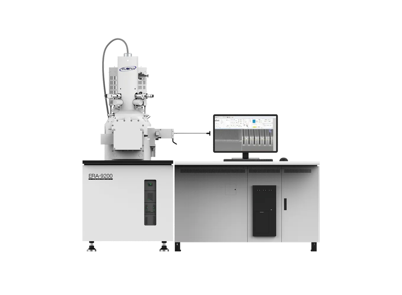
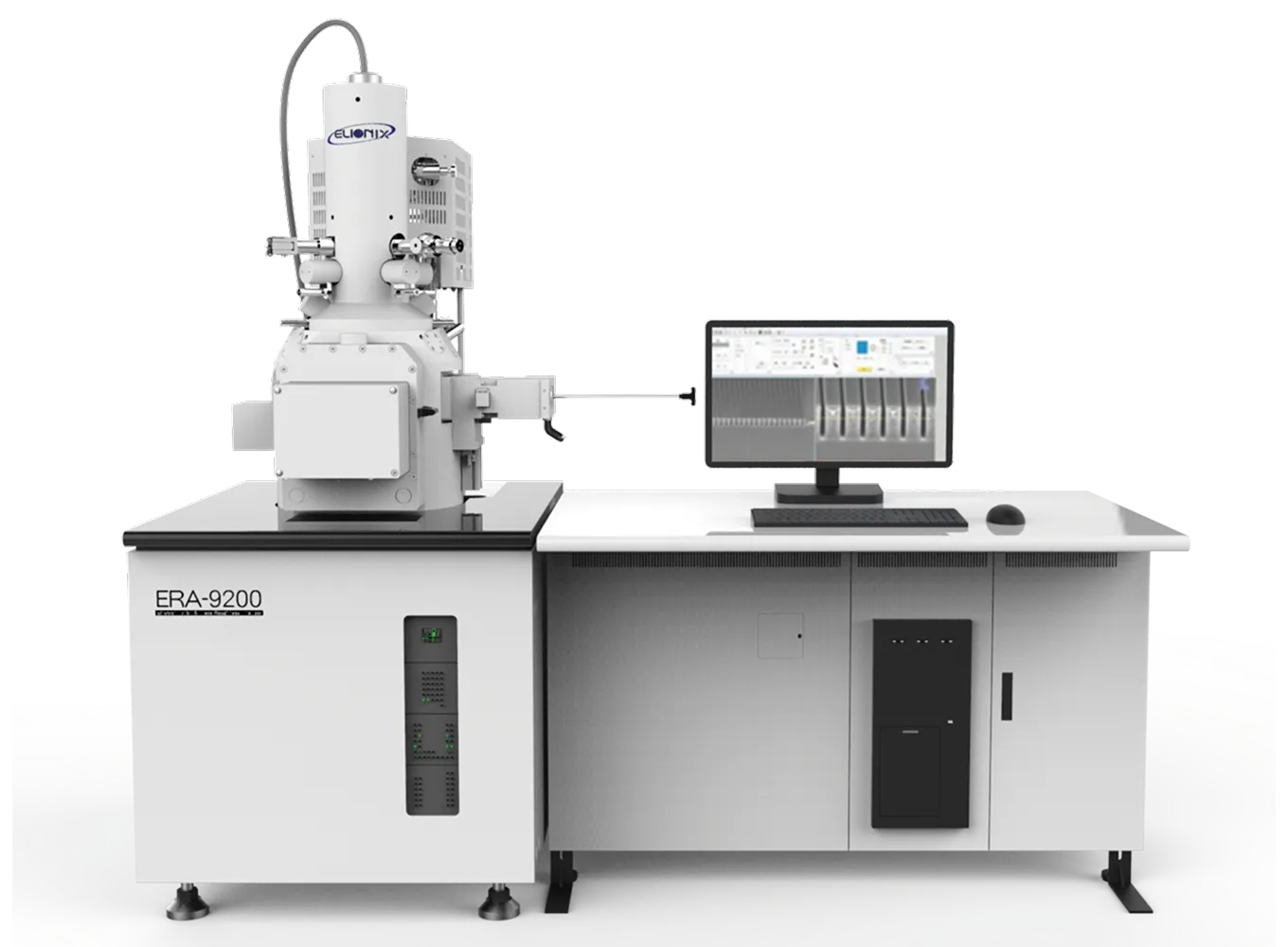
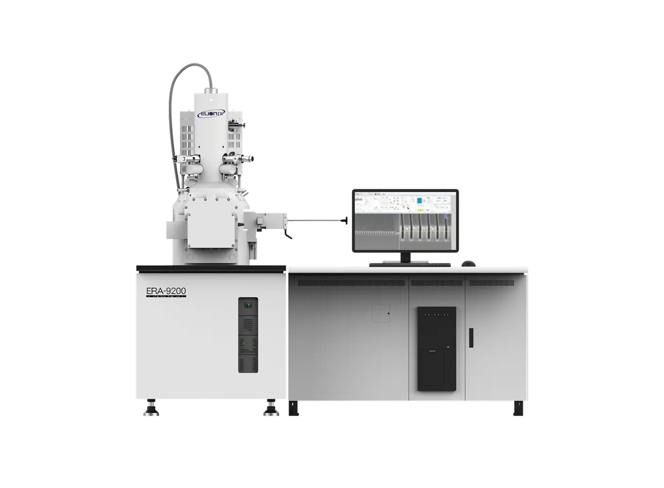
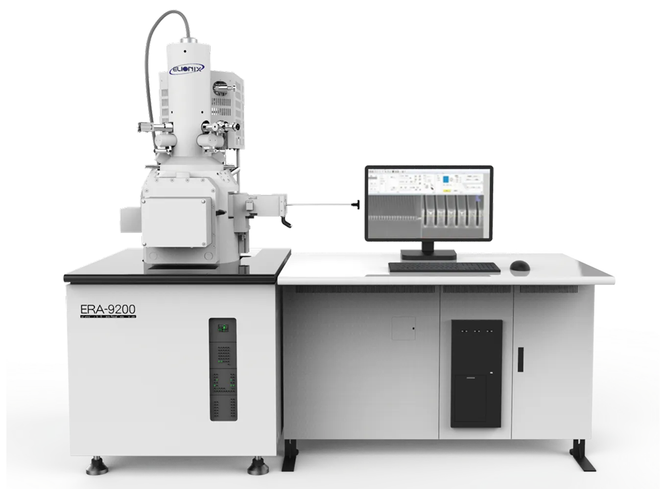
ERA-9200
【To customers considering the ERA series】
Notice of Order Suspension
Electron Beam 3D Roughness Analyzer
ERA-9200
- Measurement and Analysis Equipment
Key Features
Achieving ultra-high resolution, low acceleration, and 3D measurement at the sub-1 nm level!
We have successfully implemented shape analysis using a semi-in-lens SEM.
By enabling 3D measurement using the semi-in-lens method, we have achieved ultra-high resolution with low acceleration.
During 3D measurement, we guarantee ultra-high resolution of 1 nm in the vertical direction at a low landing voltage (voltage applied to the sample) of 1 kV.
This allows for the accurate capture and analysis of the fine topography of the sample’s outermost surface.
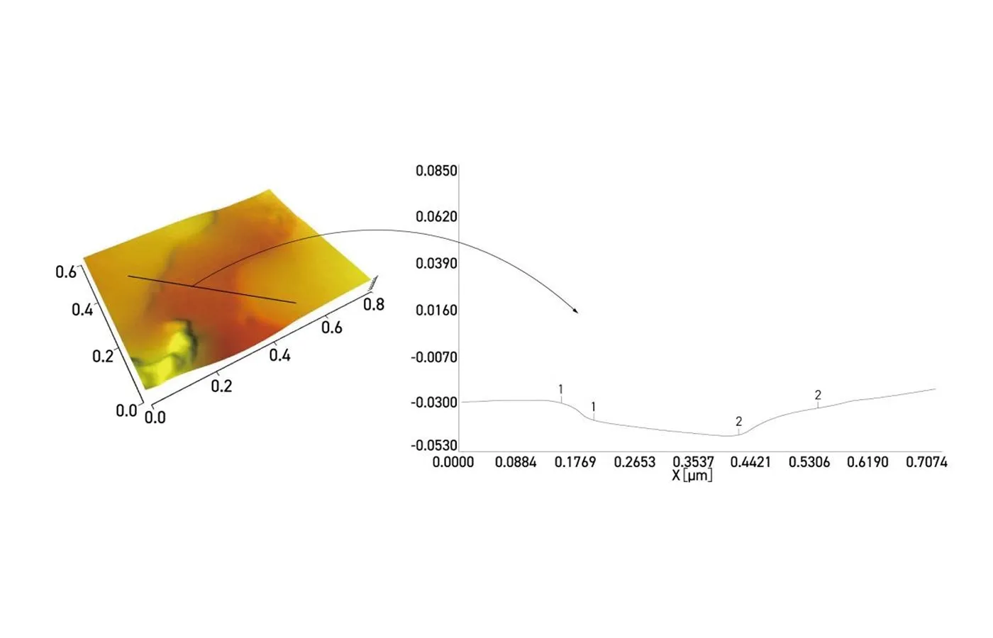
3D Shape Measurement and Surface Roughness Analysis Directly from the SEM Field of View
It is possible to acquire precise 3D shape data directly from the ultra-high-resolution SEM field of view.
The surface roughness analysis function enables the calculation of JIS and ISO standard parameters such as Ra and Rz.
Low Accelerating Voltage and High Resolution
Observation is possible at voltages as low as 100 V, and a lateral resolution of 0.7 nm is achieved at 1 kV.
By adopting a semi-in-lens system, we have achieved a maximum resolution of 0.5 nm at 15 kV.
Thorough Contamination Control
We have implemented thorough contamination control measures by adopting a dry pump (completely oil-free).
Interlock Mechanism
The system is equipped with an interlock mechanism to prevent contact between the objective lens and the sample. Additionally, a CCD monitor inside the sample chamber is included as standard equipment.
App Gallery
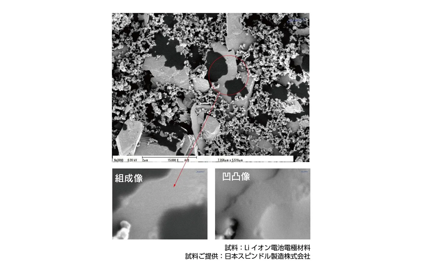
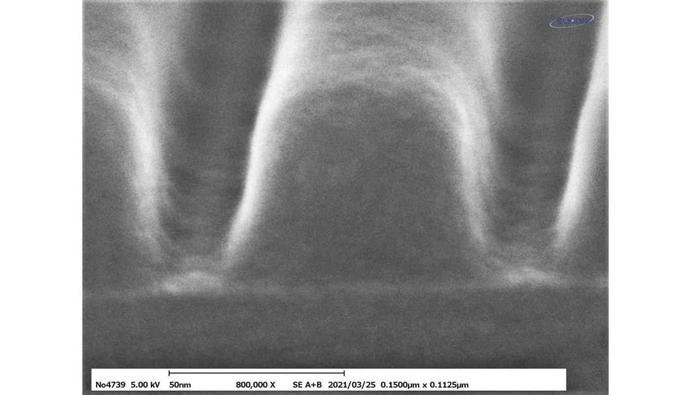
SEM image
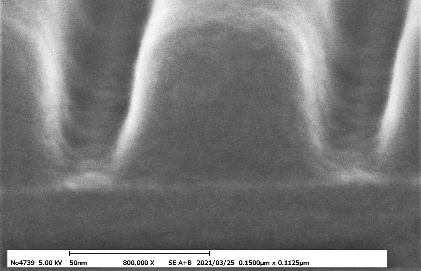
Courtesy of the National Institute of Advanced Industrial Science and Technology (800,000x magnification)
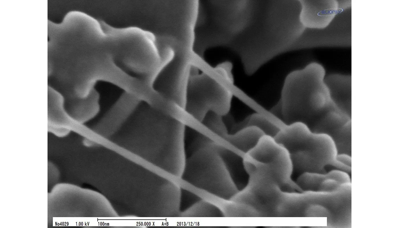
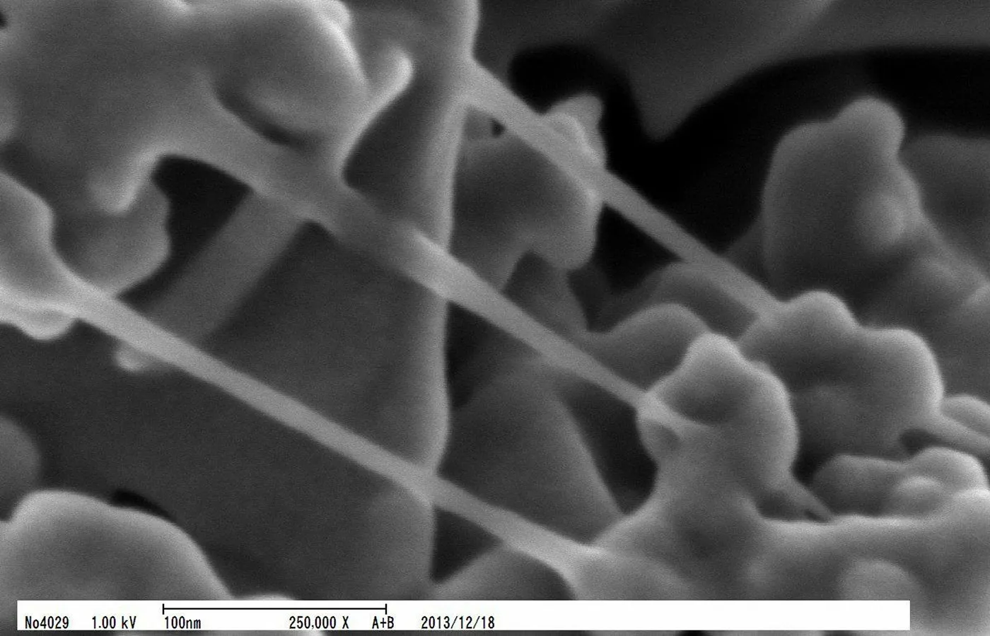
Courtesy of Nippon Spindle Manufacturing Co., Ltd. (250,000x magnification)
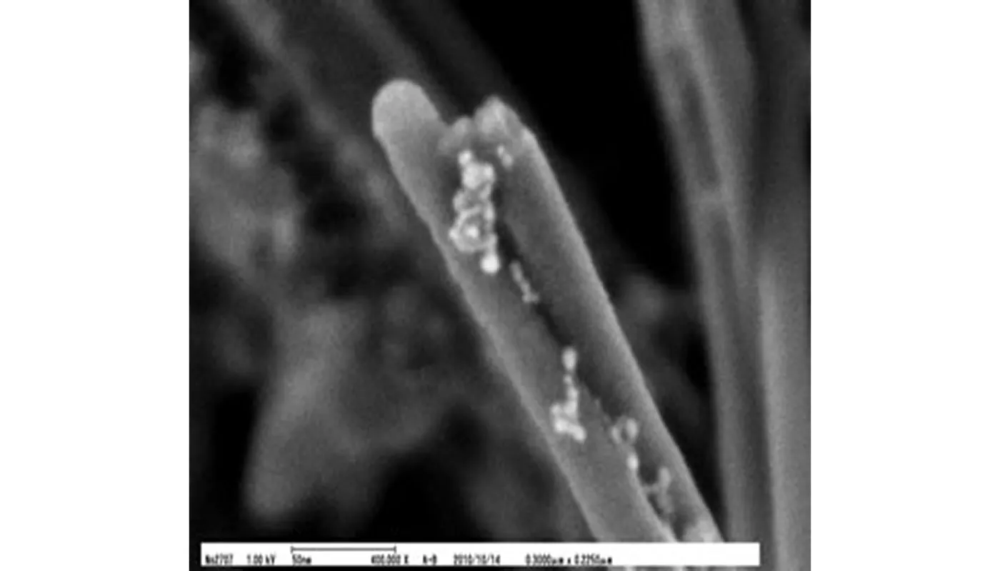
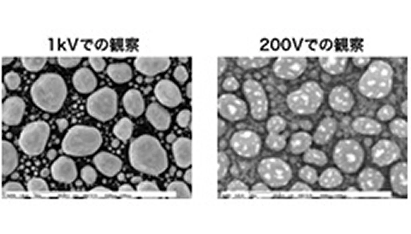
3D image
Sample provided by: Nippon Spindle Manufacturing Co., Ltd.
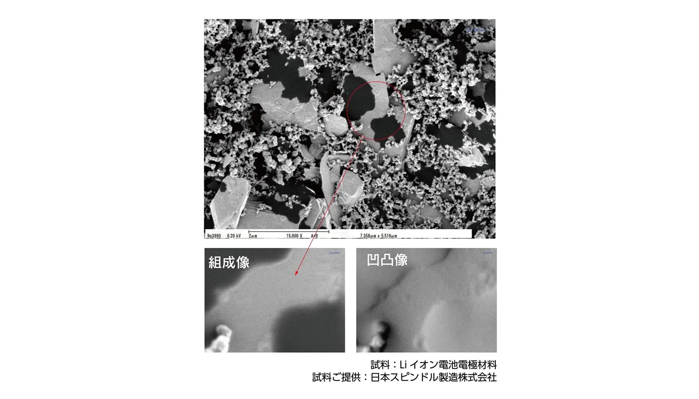
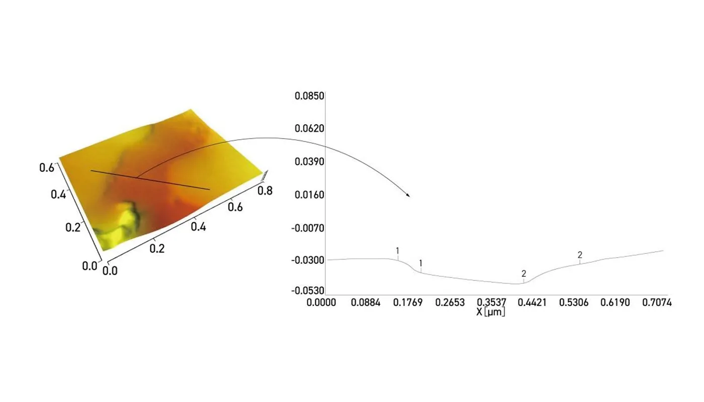
Options
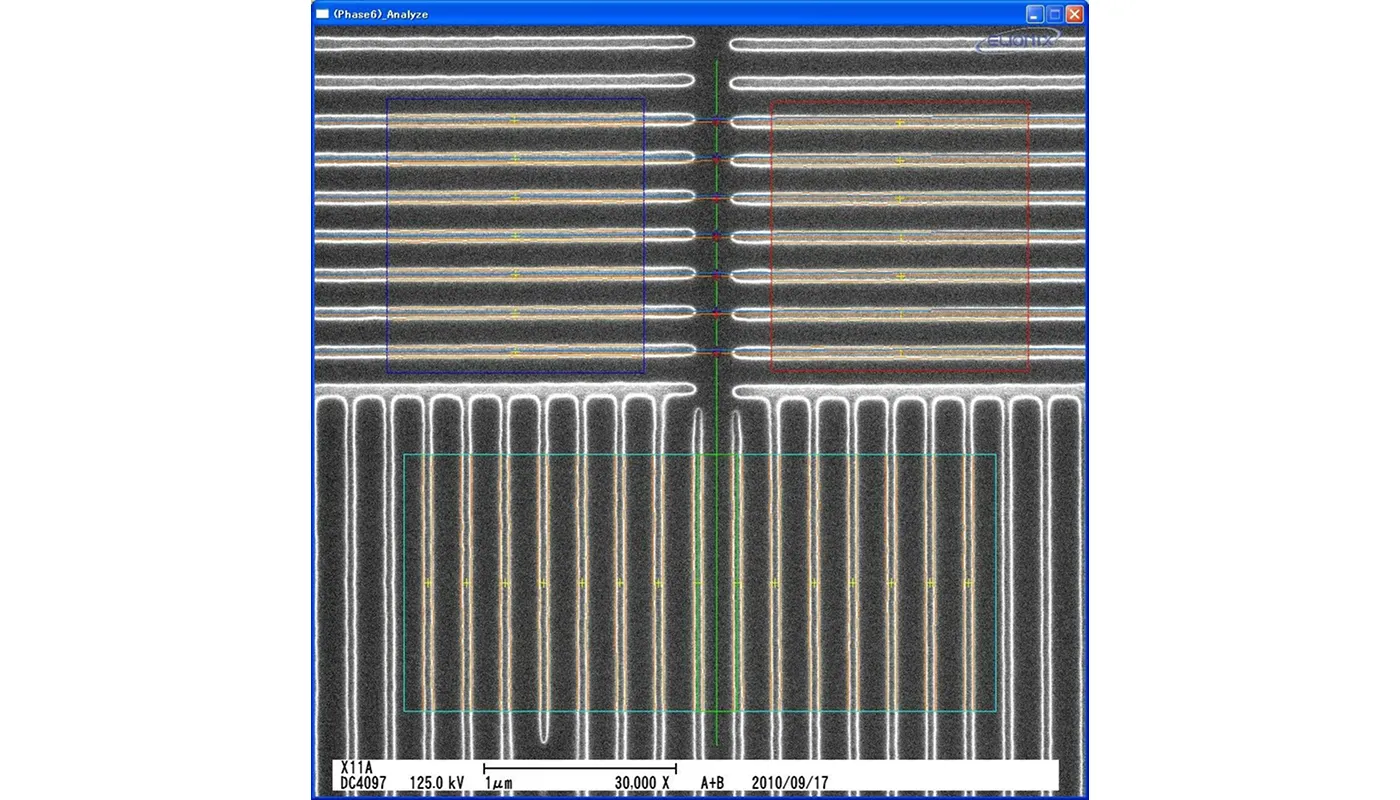
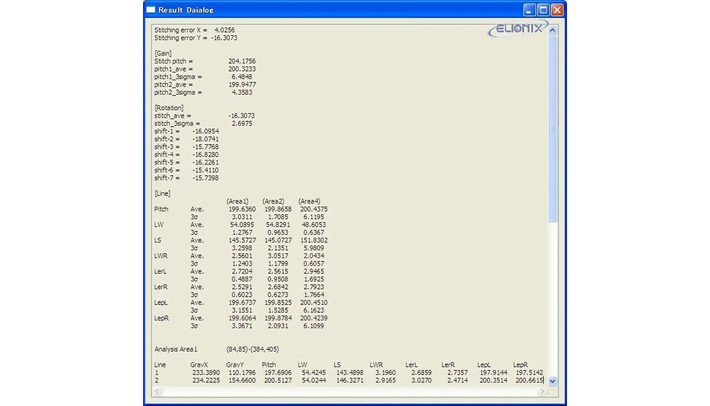
Drawing Pattern Analysis Software
This image analysis software is specifically designed for analyzing SEM images captured by ELIONIX imaging systems.
It primarily measures and analyzes SEM images containing parallel straight lines (Lines) and circular shapes arranged in a grid pattern (Dots), and analyzes the resulting data. It also allows for the evaluation of field continuity based on dedicated drawing patterns.
Key Specifications
SEM Observation System
| Electron gun | ZrO/W thermionic field emission type |
|---|---|
| Landing voltage | 100 V–30 kV |
| Secondary Electron Detectors | 4 Top Detectors 2 Upper Detectors 1 Lower Detector |
| Resolution | 0.4 nm (landing voltage 30 kV) 0.5 nm (landing voltage 15 kV) 0.7 nm (landing voltage 1 kV) |
| Magnification | 60×–3,000,000× |
| Sample Dimensions | Φ100 mm、Φ36xH10 mm、Φ26xH16 mm |
| Sample-driven | 5-axis motor drive (X, Y, Z, R, T) |
3D measurement system
| Vertical Resolution | 1 nm |
|---|---|
| Measurement Direction | X-axis, Y-axis |
| Number of Measurement Data Points |
Up to 4.32 million points |
| Data Recording Methods | Compatible with Windows |
| Analysis | Contour lines, bird's-eye view, number of peaks, area fraction of grain size, surface area, JIS standard parameters |
Applications
ERA-9200
Courtesy of the National Institute of Advanced Industrial Science and Technology (800,000x magnification)
Courtesy of Nippon Spindle Manufacturing Co., Ltd. (magnified 250,000 times)
Tip (magnified 400,000 times)
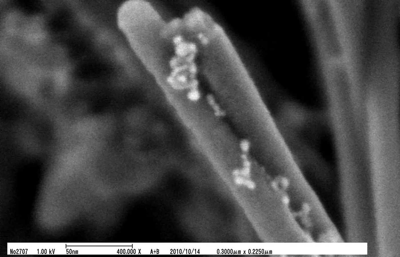
Provided by: Nippon Spindle Manufacturing Co., Ltd.