
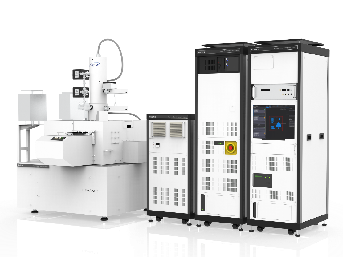
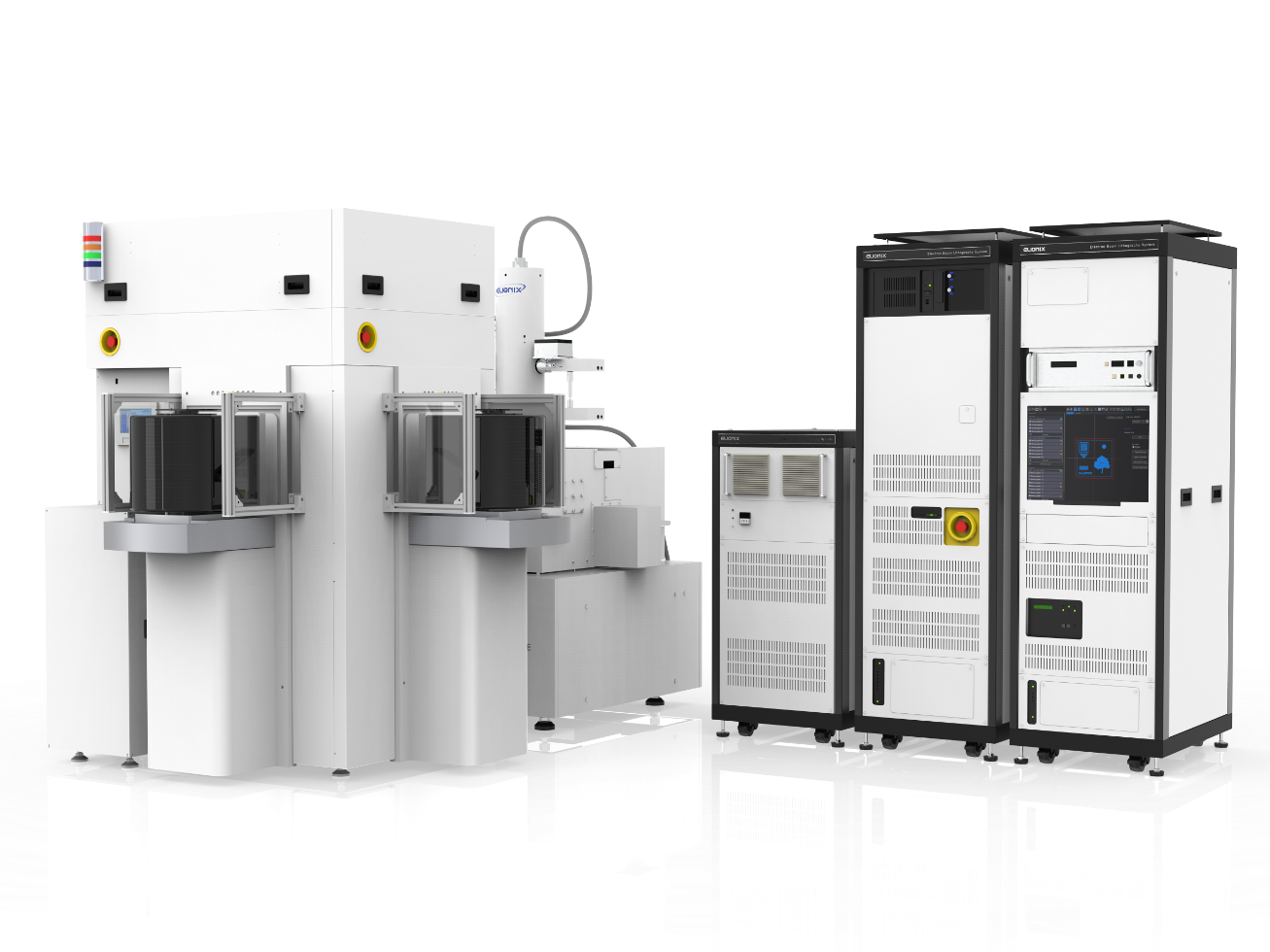
Electron Beam Lithography System ELS-HAYATE
New
Nanofabrication System
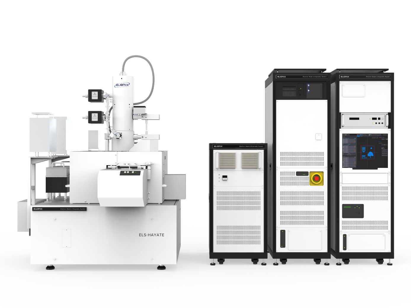
One-shot Writing with a maximum field size of 5 mm
Achieved the industry's largest 5 mm deflection. Since the area that can be written by one-shot becomes wider, it is ideal for applications where you are concerned about stitching errors between fields. In addition, as the number of stage movements within the sample surface is also reduced, it can be used for high-throughput microfabrication.
Adopts a High-Current Electron Optical System with a maximum beam current of 800 nA
Equipped with a high-current electron optical system with a maximum current of 800 nA, high-throughput microfabrication beyond the common sense of electron beam lithography is possible. Patterns on the order of µm to mm, which were previously produced by laser lithography or photolithography, can now be exposed with high quality.
Industry Fastest! 400MHz High Speed Scan Clock for Production
When lithography is performed at high current, the spot pitch had to be set wide to balance the minimum dose time and optimal dose amount. The 400MHz scan clock makes the conventional minimum dose time 1/4 in order to enable high current and narrow-shot pitch exposure that was previously impossible.
| TFE Filament | ZrO/W Thermal field emitter | ||||
|---|---|---|---|---|---|
| Acceleration Voltage | 50 kV | ||||
| Beam Current | 1 nA ~ 800 nA | ||||
| Minimum Beam Diameter | D 10 nm | ||||
| Standard Field Size | 5000 μm□ | ||||
| Min./Max. Field Size | Min. 1000 μm □ Max. 5000 μm□ | ||||
| Scan Clock | Max. 400 MHz | ||||
| Shot Ptich | Min. 1.0 nm | ||||
| Max. Sample Size | 8” Wafer / 12” Wafer | ||||
| Max. Exposure Area | 200 mm x 200 mm / 300 mm x 300 mm | ||||
| Loading Mechanism | Single Auto Loader Multi Auto Loader Robot Loader | ||||
| Software | elms • Beam adjustment function • Drawing schedule function • Pattern data conversion function • Account management • Python scripting | ||||


